Microcontact Printers for Surface Patterning and Nanoimprint Lithography
The GeSiM microcontact printers are designed to simplify prototyping of microfluidic devices and tiny 3D structures. These instruments close the gap between microfluidic research and production. They help to overcome typical design barriers:
- Photomask based lithography is expensive, each design change requires a new mask.
- Micro casting tools for mass production of disposable fluidic chips and cartridges are even more expensive.
- Biological samples quickly clog microchannels, revealing design failures and optimization needs.
GeSiM microcontact printers produce small series of tiny 3D imprints in an affordable manner. A single initial investment speeds up your R/D in the world of microtechnology.
Overview
GeSiM microcontact printers always combine two methods on one platform: a) Microcontact printing allows surface patterning down to 100 Nanometres and b) Nano Imprint Lithography (NIL) creates tiny 3D structures in polymers. Each µCP features polymer stamps with user specific patterns. An external casting station replicates consumed stamps to keep operating costs reasonably. Click the tab Procedures for details.
You are currently viewing a placeholder content from Default. To access the actual content, click the button below. Please note that doing so will share data with third-party providers.
More InformationAll GeSiM microcontact printers offer identical stamping method by pneumatic actuation and Z-movement. The compact benchtop instruments are affordable, they don’t need expensive granite beds or damping tables.
Automatic Microcontact Printers
Our automatic platforms offer programmable sequences for liquid dispensing/spinning, built-in alignment microscopes as well as unattended stamp picking/discarding for more complex applications.
µCP4.3 (Video above)
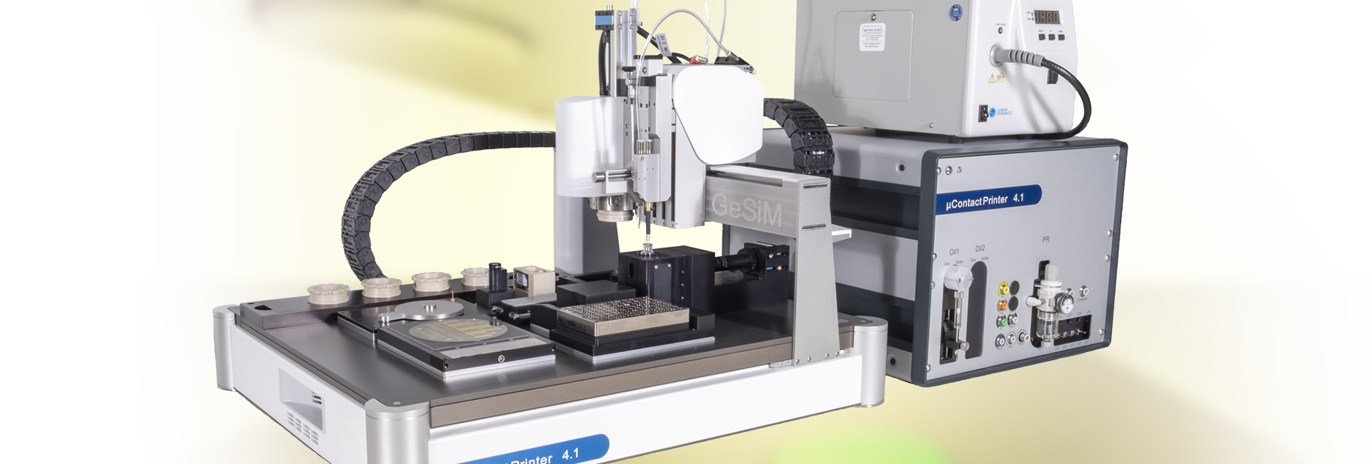
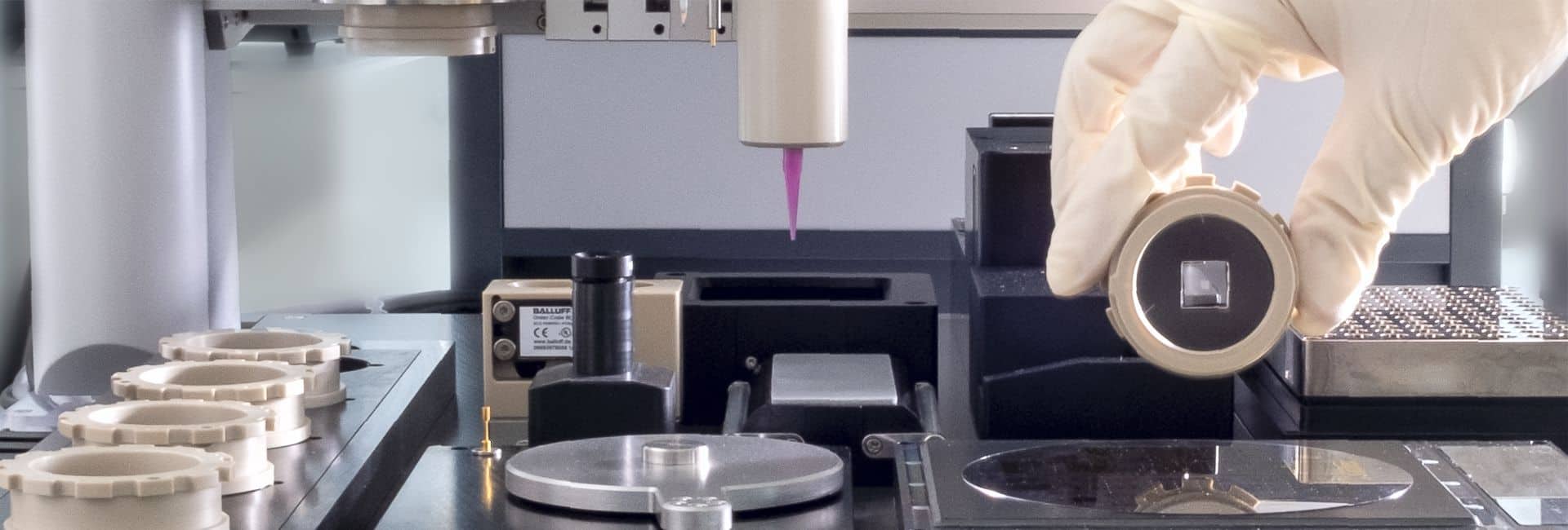
It is the most popular microcontact printer for transparent and non transparent targets (E.g. silicon wafers). It comes with alignment camera, stamp head, UV hardening and rack for up to five stamps. The max. stamp size is 20 x 20 mm. Up to five different inks/reagents can be printed by aligning all stamps to specific fiducial markers on the target.
µCP6.3
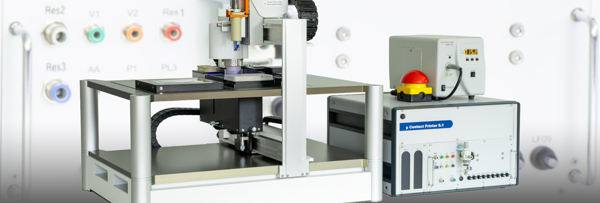
The automatic micro-contact printer has a two-level working tray which makes it perfect for UV transparent print targets. The UV source is arranged on the lower level, opposite to the print stamp on the upper level. A collimator combined with a photomask synchronizes the exposition frame perfectly to the stamp image field. This method allows multiple imprints on one target up to six inches without spacing between adjacent images (“Chessboard” style). With a patterned photo mask in the UV beam, two lithography steps at once (Photolithography and stamping) become feasible. It allows to create more complex designs in one step, e.g. tiny pillars in the centre of a microfluidic channel.
µCP6.3/E
Same as before, a larger work tray adapts more targets for batch processing. All µCP6.1 instruments feature powerful but silent and precise linear motors.

µCP4.3 does single or multiple prints with spacing in between (Left); µCP6.3 is capable of perfectly matched “chessboard” prints (Middle); The collimator optics of µCP6.3 (Right) combines photolithography with nanoimprint lithography
- Stamp rack for up to five individual stamps
- Alignment microscope
- Pneumatic cartridge dispenser
- Spin coater
Options:
- Pipetting unit, operating either piezoelectric Nanolitre pipets or standard pipet tips for the Microlitre range
- UV-lamp
- Cartridge heater
- Heatable substrate table
Semiautomatic Microcontact Printers
Here we present solutions for low-throughput research, without the need of automatic tooling and alignment.
µCP Core
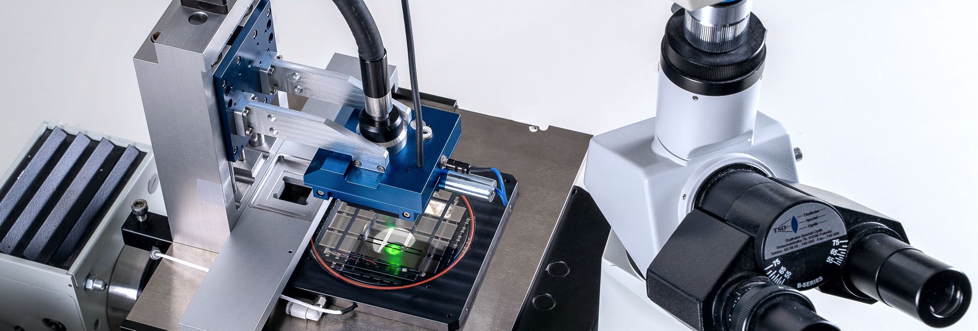
This entry-level microcontact printer offers attractive price and manages just one stamp. It fits on the stage of most popular inverse microscopes. Stamp alignment is than done by the microscope table instead of the GeSiM printer. Accessories like UV-lamp and temperature control module are available. As for the automatic printers, µCP Core uses stamps of two sizes: 20mm x 20mm and 10mm x 10mm.
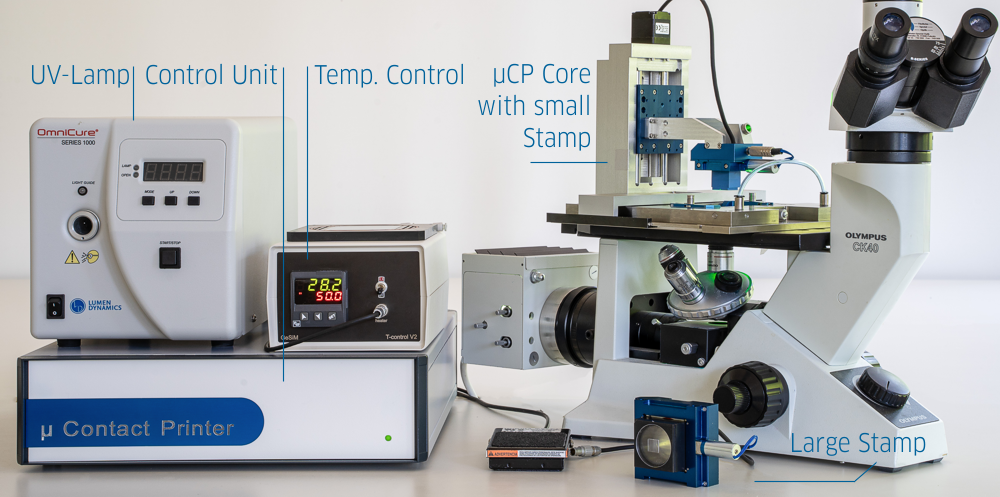
µCP Core (right) on a microscope stage.
Microcontact Printing With the GeSiM Polymer Stamps
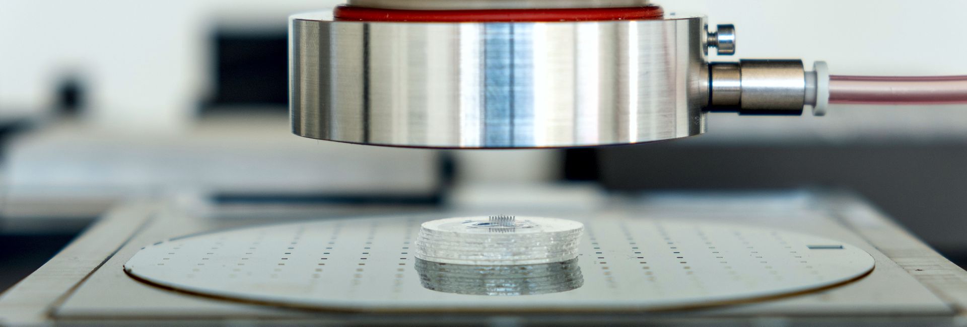
Whether you decide for an automatic solution or for the entry-level µCP Core, the stamping module is always the same. The clever combination of pneumatic actuation and Z-movement ensures high reproducibility for patterns down to the range of 100 Nanometres.
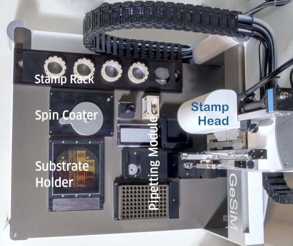
Layout of µCP4.3 with optional pipetting unit – An automatic benchtop robot
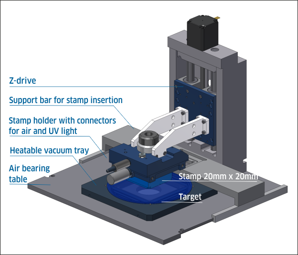
Components of µCP Core – Requires an inverse microscope as well as a UV lamp (Not included)
Our Microcontact Printer for your Individual Research
The particular foot layout of the polymer stamp is always the specific link to your daily research routine. A typical startup incorporates the following steps:
- An application test with your material will be done at GeSiM if necessary. Feel free to contact us.
- Based on your unique print design(s) GeSiM develops one or several silicon master chips.
- Each GeSiM microcontact printer comes with a small casting station to produce copies of the sensitive stamp(s). Thus, your operational costs remain reasonably even when your process requires “fresh” stamps very often. During the design optimization new silicon masters can be ordered at GeSiM.
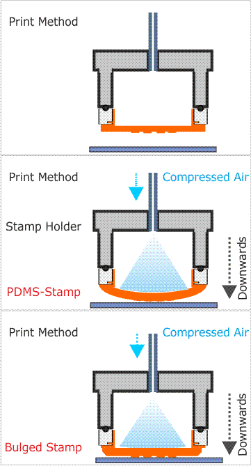
Basic function of all GeSiM microcontact printers
The footprint of the stamp represents particular patterns down to 100 Nanometres. Both PDMS and PTFE are proven polymers for these stamps. The complete process differs for microcontact printing and NIL (See next tab). Both SU8 and NOA 81 (Norland) are popular resists for 3D imprinting.
When the print head touches down the stamp gets bulged out by air pressure and connects smoothly and without artefacts to the substrate surface. Onboard video microscopes on the automatic printers allow X/Y/Phi alignment of the stamp to existing patterns or markers on your target object.
Fluidic “flow-through” stamps are a special version for applying grains or bead during the microcontact printing process.

Different sizes of PDMS stamps for GeSiM microcontact printers
Optional Tools for Material Handling on µCP4.3 and µCP6.3
All automatic GeSiM microcontact printers come with built-in spinning table and a pneumatic cartridge dispenser. It allows to create homogeneous resist layers for precise NIL. Our optional tools allow selective coatings and the application of multiple materials on the target:
- Displacement pipet tips as you use it in your daily work flow
- Piezoelectric GeSiM dispensers for managing smallest volumes
- Piezoelectric valves (Third party) for making smallest drops of high-viscous liquids.
- Powder pipets for transfer of micrograms of granular materials.

µCP stamp (Left) and powder pipet above a reservoir (Right)
UV Lamp
The UV lamp for resist hardening is available for all automatic microcontact printers but optionally available for µCP Core.
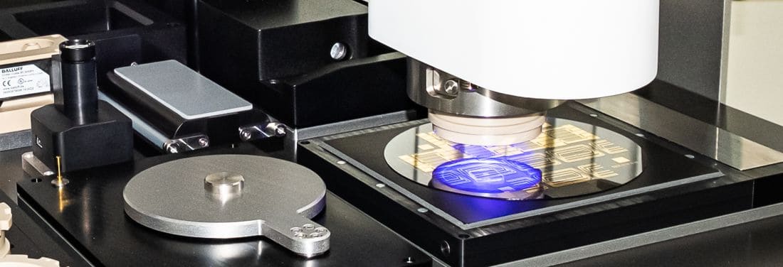
UV hardening during NIL on µCP4.3
Each GeSiM microcontact printer allows two different applications:
Microcontact Printing
This process transfers a sample liquid called “ink” onto a planar target surface. The PDMS stamp is inked with the sample, subsequently pressed onto the surface, thereby transferring the sample only from the high areas, as in letterpress printing.
Spinning of ink on target
Stamp inking
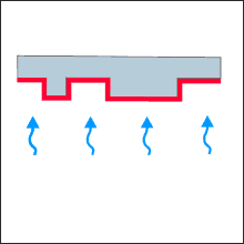
Drying of Stamp
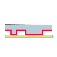
Stamping
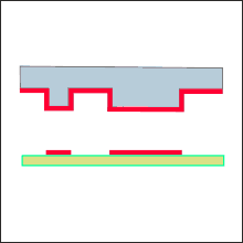
Stamp detached from target
Not just chemicals, also biomolecules, nanoparticles, beads, or cells can be printed. Patterns of proteins like fibronectin or laminin can serve as adhesive substrate to grow cells only on protein-covered areas.
GeSiM printers automatically use up to five stamps with different inks and different patterns for well aligned prints on the same substrate.
NIL – Nanoimprint Lithography
Nanoimprint Lithography (NIL) is a popular approach to make disposable microfluidic devices at low numbers. The GeSiM microcontact printers have to be supplied with a curable photopolymer as well as with the printing substrate.
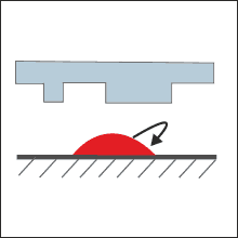
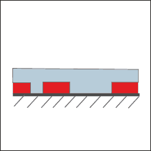
First, the target surface has to be coated with an appropriated material, e.g. a liquid, UV-hardened, polymer. Then, instead of transferring an ink, the elevated patterns of the PDMS stamp shape their reverse image into a homogeneous layer on the stamp target. µCP6.3 is capable of lining up several prints step-by-step without any spacing in between.
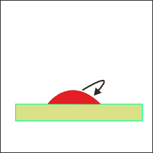
Spinning of photo resist
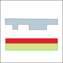
Stamp alignment/ Drying
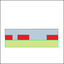
Stamping
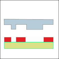
Stamp detached from target
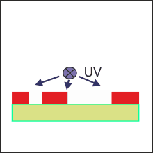
UV hardening
3D structures can be printed with SU8 photoresist or NOA (Norland). Heights of up to 150 microns are feasible. The aspect ratio height/width depends on the layout but can easily reach (3…5)/1.
After detaching the stamp the printed targets can be sealed by cover lids in order to achieve microfluidic devices.
Content
- Selection of Applications Already Done
- Micro-Contact-Printing: Fibronectin Patterns Printed with µCP
- Nano-Imprint-Lithography: Micro Needle Arrays
- Nano-Imprint Lithography: Nanoplasmonic Sensor Structure by NIL
- Nano-Imprint Lithography: Picolitre Wells for Cell Biology
- Nano-Imprint Lithography: NIL of Micro Wells with Interconnecting Channels
Selection of Applications Already Done:
- Selective printing of self-assembled monolayers (SAM) by µCP, or microstructuring by NIL, on metal (Cu) and electroplating on the unprotected areas
- Fabrication of silver micro- and nanopatterns by µCP of SAM on glass and electroless metallization
- Direct (nano)imprinting of microfluidic structures into photoresist
- Microcontact printing of extracellular matrix proteins to direct cell adhesion to certain spots (see below…)
- Fine-structuring of surfaces via NIL for cell growth studies (e.g. flat vs. grooved surface)
- Printing of patterned thermoresponsive microgel coatings to study adherent cells (Uhlig et al., 2016)
Micro-Contact-Printing: Fibronectin Patterns for Cell Growing
Human Umbilical Cord Blood Neural Stem Cells (HUCB-NSC) were grown on microcontact printed fibronectin squares for a differentiation study.
The squares were printed using PDMS stamp on a cell repellent, plasma polymerized poly-ethylene-oxide (PEO) like surface using fibronectin solution in an acetate buffer as an ink.
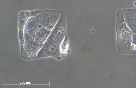
HUCB-NSC cells on micro-contact printed Fibronectin squares – Phase contrast image
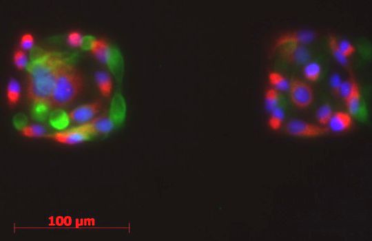
Fluorescence Image – Green: β-tubulin-II neuronal marker; Red: GFAP; Blue: Cell nuklei
The cells do not adhere to the PEO coated regions, but are attached to the printed 100 µm fibronectin squares. After the culturing period the cells were fixed and immunostained for glial and neuronal differentiation markers.
Courtesy of EC Joint Research Centre, Nanobiosciences Unit, Ispra, Italy (Dora Mehn)
Nano-Imprint Lithography: Micro Needle Arrays
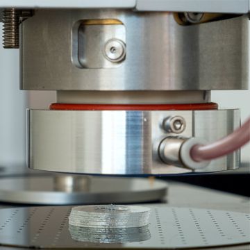
Vacuum containment on the print head of µCP4.1
Functionalized micro needle arrays gain increasing interest for subcutaneous drug delivery without injection needles. Development of a cost-effective manufacturing technology for controlled drug release is still challenging. Here we present an approach for low-volume manufacturing of micro needle arrays with the GeSiM micro-contact printers. Nano-Imprint-Lithography allows much better spatial resolution than conventional 3D-SLA.
Microneedle arrays with high-aspect ratio are achieved by evacuating the space around the PDMS stamp. GeSiM microcontact printers are available with a containment ring surrounding the stamp. Thus a sealed volume allows evacuation when the stamp touches down on the print target.
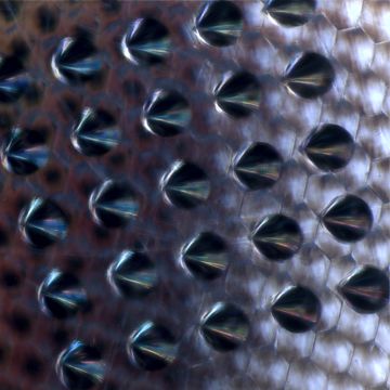
Master structure for stamp casting
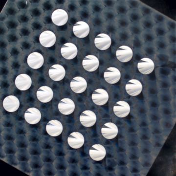
PDMS print stamp
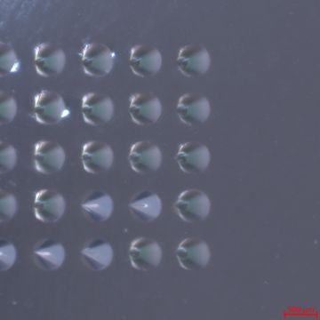
Final micro needle array
The master structure for multiple stamp casting (left(top) image) was done by 2-photone-lithography using a stiff synthetic material. The µCP4.1 stamp was than made from PDMS Sylgard 184, Dow Chemicals Europe GmbH) as usually (middle). Finally the micro needle array (right (bottom)) consists of a UV-hardened resist (NOA-63, Norland Products Ltd.).
The geometry of the NOA-63 needle array supports usability: The height is 1,200 µm, both bottom diameter and spacing between adjacent needles are 200 µm.
For more details please download the µCP4.1 microneedle array application note.
Nano-Imprint Lithography: Nanoplasmonic Sensor Structure
Surface plasmon resonance (SPR) sensors allow label-free, real-time biomolecule detection with high sensitivity. Classical SPR sensors utilize a gold film on a prism, which cannot be scaled down. To overcome this, a nanostructured gold layer is used to excite plasmons without bulky optics. The nanoplasmonic sensor structure detects diclofenac in wastewater using immobilized diclofenac in the presence of diclofenac antibodies (Steinke et al., 2018) or measures ethanol concentration during fermentation processes with an ethanol-sensitive hydrogel (Kroh et al., 2019).
Central to this method is the reproducible fabrication of nanostructured surfaces by nanoimprint lithography (UV-NIL) using a GeSiM µCP 4.1 and a UV-cross linkable photoresist.
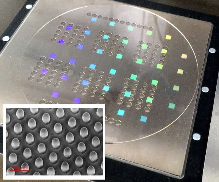
Nanopillar arrays made by UV-NIL on a glass wafer with a GeSiM µCP4.1, SEM image inline
Nano-Imprint Lithography: Picolitre Wells for Cell Biology
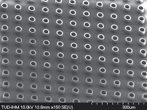
Picowells, 25 µm wide, printed by UV-NIL, empty
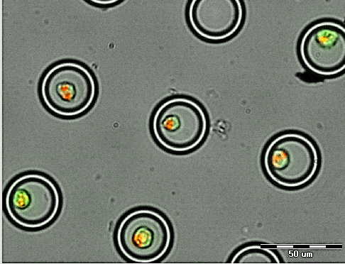
Picowells filled with cells
In cooperation with M. Deutsch’s lab from Bar-Ilan University and others, picowell arrays have been printed by UV-NIL in UV-curable adhesives such as NOA81 for the activity measurement, e.g. by multiparametric enzymic assays, of individual cells (Deutsch et al., 2010; Afrimzon et al., 2010; Markovitz-Bishitz et al., 2010).
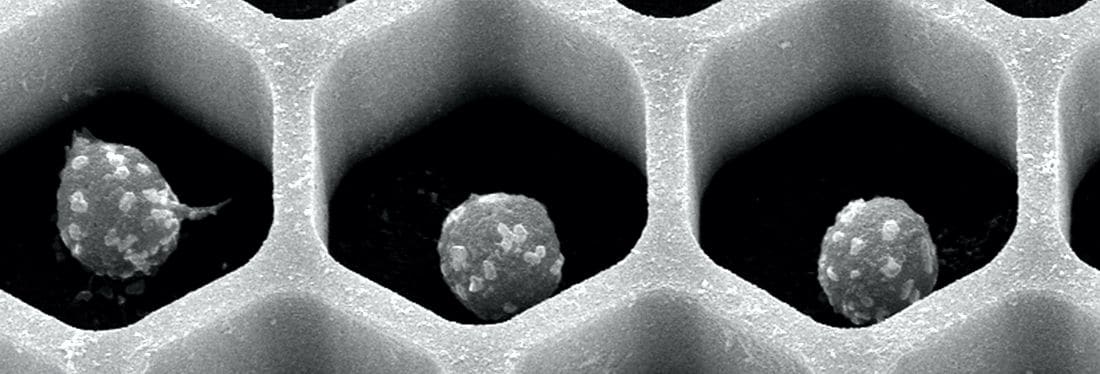
NIL made honeycomb Picowells with single cells
One application was toxicology testing of nanoparticles that the GeSiM Nano-Plotter had spotted into the picowells, another the formation and study of organoids from cancer cells in honeycomb structures (Zurgil et al., 2014), also with electrodes.
Courtesy of Matti Deutsch, Bar-Ilan University
Nano-Imprint Lithography: In Vitro Neurotoxicity Assay Development
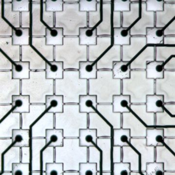
Electrodes on the well bottom of a MEA chip, each well 100 x 100 x 50 µm
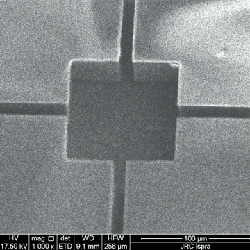
Scanning electron microscopic image of one well of the microarray (by Cesar Pasqual Garcia)
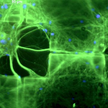
Primary (rat) neurons grown forming a network in the microwells; Green: β-tubulin-II neuronal marker, Blue: cell nuclei. (by Jakub Nowak)
Microelectrode array chambers (MEA chips) were applied as a support to generate 3D microwell environment for neural cells in electrical activity measurement studies.
The printer with UV illumination and the 24 well stamps were used to generate imprints with 100 µm sized wells and interconnecting channels aligned to the electrodes of the multi-electrode arrays. The matrix of PEG based hydrogel was polymerized by 60 s UV exposition.
Courtesy of EC Joint Research Centre, Nanobiosciences Unit, Ispra, Italy (Dora Mehn)

