Microfluidics – Services for Design, Manufacturing, Instrumentation
Integrating the Worlds of Micro- and Macrotechnology
Wether you need just a cell friendly coating on your slides or a complex automatic lab: GeSiM is your one-stop shop for instrumentation in life science. Our expertise is based on more than twenty years engineering of microfluidic systems. Our strength is the completion of these small components with powerful robots, innovative software and “classical” lab hardware (pumps, valves).
Here we present a fully automatic lab for culturing of cells and organoids. The next tab “3D Structuring” outlines basic services for customized microfluidic flow-through cells. “Chips & Services” is your source of information for specific engineering services.
Please don’t miss the MicCell, a separate GeSiM product line for polymer microfluidics with microscope interface.
Microfluidic Multi Cell Cultivation with Automatic Sample Handling
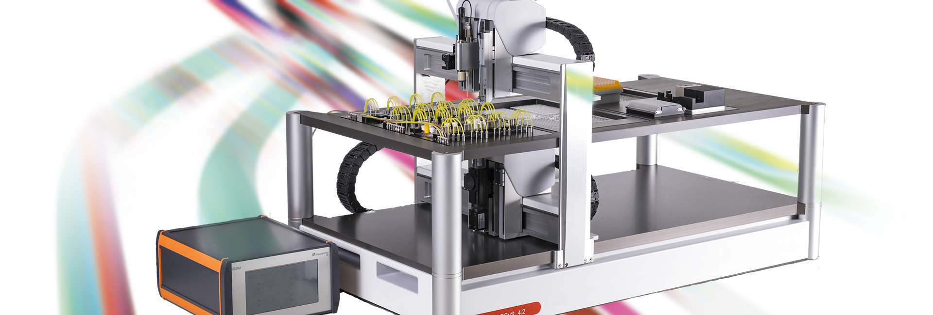
The Microfluidic Workstation (MW) is a benchtop robot with “flying” work deck. It is made to operate small transparent bio containments, e.g. SBS well format objects, microfluidic cartridges and others. It features two tool heads for optical inspection in both directions. The upper tool head operates all GeSiM made tools for liquid handling, Nanolitre pipetting and paste dispensing. Full 3d printing is given by the modular approach of GeSiM instruments. The recesses of the work decks accept carriers for arbitrary target formats.
The MW can be configured for applications like in-vitro tissue engineering, multi-cell cultivation, single cell handling and microarraying. It fits into biosafety cabinets. Other safety enclosures are available on request.
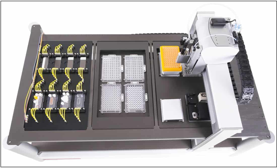
Microfluidic Workstation: Elevated “flying” work deck with trays for multi-organ-chips (left) and 96well plates (middle)
The configuration above accommodates an array of Multi-Organ-Chips (MOCs) on the left tray. Each MOC hooks up to a separate control unit for media and temperature adjustment. The MOC design can be adapted to different applications. For more details on the MOCs please click the tab “Applications”. The MOCs resulted from a joint research project with Fraunhofer IWS, Dresden.
Examples of MOCs:
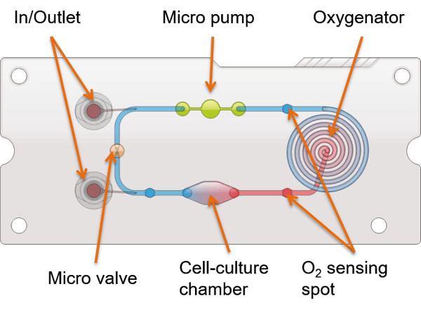
Hypoxia assay
Hypoxia Assay
- Oxygen control directly on culture media
- External gas mixer
- Gas permeable membrane for in/output
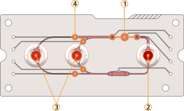
Systemic toxicity assay
Systemic toxicity testing
- Two parallel-connected cell culture chambers (3), reservoir (2)
- 3-point-peristaltic-pump (1), inlet and outlet valves (4)
- Temperature controlled support
The measurement cameras can be configured to different detection methods, e.g. fluorescence microscopy, phase contrast microscopy and turbidity measurement for ELISA.
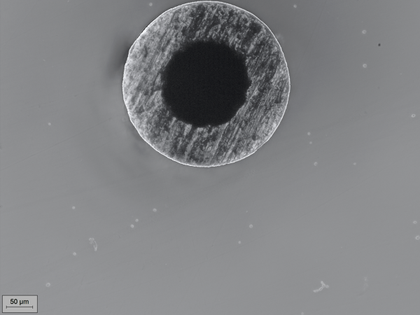
Yeast cells in a SBS well plate – bottom view. The picking capillary orifice is at the upper edge.
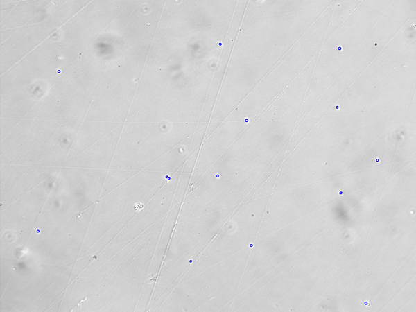
The software of the MW recognizes single cells, differentiating from optical artefacts.
Sandwich Structures for Microfluidic Manifolds
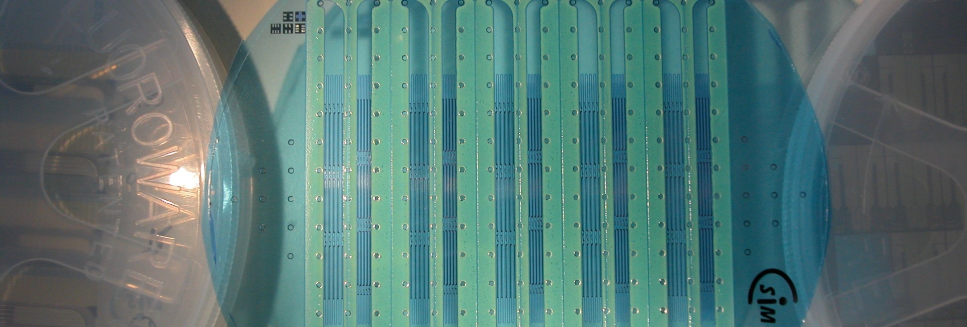
GeSiM offers different approaches for micromachining of 3D structures. Microfluidic devices are easily made from silicon/glass sandwiches. However, many applications require optical transparent channel structures. Glass/glass sandwiches are precise but more expensive and give high accuracy.
PDMS microfluidics keeps prices close to disposables but requires more initial instrumentation. Please refer to the GeSiM MicCell or even the Micro-Contact-Printers. The latter one prints your microfluidic devices (NIL – Nano-Imprint-Lithography) including sample handling by onboard pipettors.
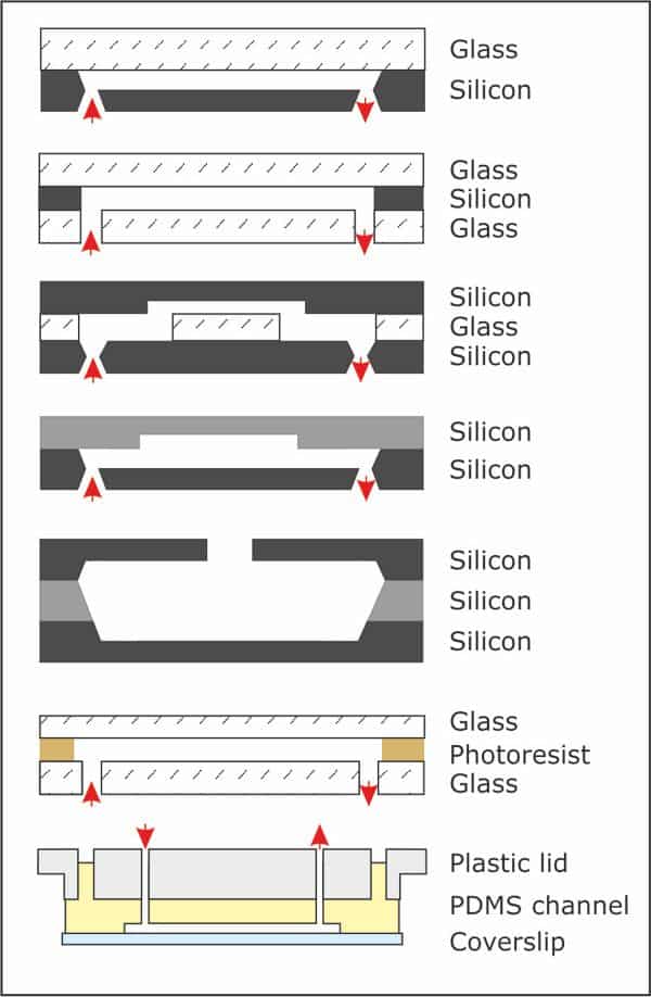
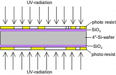
Different sandwich methods for microfluidic devices
3D Microfluidics from Hard Materials
- Anisotropic wet-chemical etching of Si with KOH: inexpensive batch process, smooth surface, side wall angle depends on crystal orientation
- Anisotropic plasma-enhanced dry Si etching (ASE/Bosch process): single wafers, dense structures, vertical side walls
- Super-rough surfaces by etching in SF6/C4F8 plasma
- Isotropic wet etching of glass with HF: round channels, 3 – 700 µm deep
- Ultrasonic drilling and micro-blasting for 150 – 1000 µm thick glass, Si, quartz
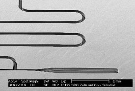
Etched channel structure of a micromachined sieve
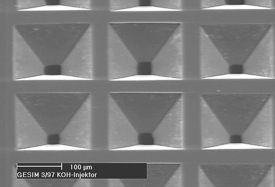
KOH etched sieve structure
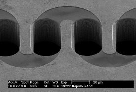
Micro pores, realized by ASE at presence of insulated platinum electrodes
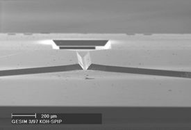
GeSiM dispenser structure: View from the pump chamber of the fluid inlet
Photoemulsion Masks with your Design
We supply cost effective photo emulsion masks for patterns down to 25 microns. Smaller features are available with chrome masks from an external source. The photo emulsion masks are based on glass substrates 5″ x 5″ as well as on films of diverse sizes.
If desired we also offer CAD services for your particular application.
Technical Information on the GeSiM Mask Service
We accept CAD data accordingly to the following rules, as well as create plot files based on your specs.
Supported data formats
- AutoCAD™ DXF up to release 12 (preferred),
- Gerber RS 274X,
- GDS-II, CIF.

Lithography equipment (Left), photoemulsion mask (Right)
Design guidelines
For 5” masks, the plotting area is restricted to 100 mm x 100 mm. For a centered image on the mask, the outer dimensions of the drawing must be exactly 100 mm x 100 mm. Placing of four small squares (e.g. 50 microns x 50 microns) in the corners of the layout supports this contraint.
In DXF files, please use only solids, circles and closed polylines with a width of zero. These patterns will be filled by our software. Do not try to fill them with the hatch command. Avoid “islands”, try to split complex figures in separate parts instead. For text information, use only the text command, never dtext or mtext. Please set the font to txt.shx.
Download our sample file as a design template.
Thin Film Services – Coating Technologies
GeSiM offers the deposition of conducting and insulating films by
- Physical Vapor Deposition
- Plasma-Enhanced Chemical Vapor Deposition
- Screen Printing
Physical Vapor Deposition (PVD) by Magnetron Sputtering and Electron Beam Deposition
Can be applied to different materials:
- Conductive materials: Aluminum (Al), titanium (Ti), platinum (Pt), tantalum (Ta):- Thickness from 0 to 200 Nanometers.
– Resistance in the micro ohm range.
– Patterning by lift-off and etching technologies.
– Single-layer or multi-layer coating of these materials. - Conductive and transparent material ITO-90/10 (90% indium oxide In2O3 and 10% tin oxide SnO2):
– Thickness from 20 to 200 Nanometers.
– Resistance from 30 to 50 Ohm.
– Patterning by lift-off and etching technologies. - Evaporated quartz SixOy, coated at 150° C.
Plasma Enhanced Chemical Vapor Deposition (PECVD)
- Silicon oxide SiO2, silicon nitride Si3N4 and low stress oxinitride SixOyNz as alternative insulator materials:
– Thickness from 20 Nanometers to 1.5 Microns.
– Patterning by RIE dry etching and wet chemical etching. - Hydrofluorocarbon CxFy layers. Material similar to Teflon®:
– Thickness range from 50 Nanometers to 2 Microns.
– Patterning by O2 RIE plasma etching.
PVD and PECVD applies to all kind of substrates up to 4 inch diameter.
Screen Printing
- Dispensing of the state of the art adhesives on printed circuit boards and micro system substrates for surface mounted device packaging.
- Dispensing of silicon rubber.
- Includes sieve design and production.
- Typical thickness of printed materials in the range of 15 to 35 Microns.
Bonding – Connecting Microfluidic Chips with and without Glue
In order to achieve closed fludic channels MEMS technologies offers different – material dependent – methods. The GeSiM engineering service covers:
- Anodic bonding
- Silicon fusion bonding
- Die bonding using adhesives
- Wire bonding
Anodic Bonding
- This process generates very tightly connected layers, produced by the application of high voltage and high temperature, and is ideal for the irreversible covering of microfluidic channels.
- Bonding of double and triple sandwiches of silicon and Pyrex glass
- Maximal substrate diameter: 4 inches (10 cm)
- Process temperature between 300°C and 450°C.
- Bonding with or without prealignment. Aligning accuracy ≥ 5 microns.
- Bonding of insulator (Silicon oxide SiO2 or Silicon nitride Si3N4) silicon surfaces.
Silicon Fusion Bonding
- Adhesive bonding after wet chemical pretreatment of substrates in strong acids
- For double sandwiches of (micro-machined) silicon
- Maximal substrate diameter: 4 inches (10 cm)
- Process temperature between 950°C and 1100°C under nitrogen atmosphere
Die Bonding Using Adhesives
- Computer Aided Design and sieve production for screen printing of adhesives
- CAD and preparation of polymer spacers
- Adhesive die bonding on whole wafers or on single chips
- Aligning accuracy ≥ 5 microns
- Usage of conductive adhesives to interconnect electrodes of top and bottom substrate of the die bonded sandwich
Wire Bonding
- On or between glass, silicon, ceramic, printed circuit boards with metal bond pads.
- Wire material AlSi1, diameter: 25 microns.
- Minimal bond pad area 30 x 30 microns².
- Sealing of bond wires with epoxy.
Wafer Dicing Service
GeSiM accepts flat wafers with diameters up to 6 inch, furthermore tubes and objects of other geometries (please ask).
Substrate Materials
- Silicon (up to 2 mm thick)
- Different glasses (up to 1.5 mm thick)
- Different Ceramics (up to 1.5 mm thick)
- Stainless Steel (up to 1.0 mm thick)
Support
- Pressure sensitive tapes
- UV-curing tapes
- Dicing wax
Instrumentation Service for R/D – Integrating the Worlds of Micro and Macrotechnology
The exchange of material and information with MEMS is more complex than with standard microelectronic chips. GeSiM offers customized solutions for packaging, liquid handling and instrument design.
- Hybrid integration of Si or glass chips in ceramic of other wire bonding mounts,
- Innovative electrical, fluidic and mechanical joining technology,
- Integration of macrofluidic components (E.g. valves, pumps) or custom-specific parts,
- Development of hard- and software,
- Customization of GeSiM standard instruments.
Further MEMS Services
Microgalvanics: Galvanic deposition of thick layers of Ni (70 µm), Au (70 µm), Au (10 µm), after lift-off microstructuring
Screen Printing:
- Printing of SMD adhesives or silicone rubber on PCBs and microsystem substrates
- Including sieve design and production
- Typical thickness: 15 – 35 µm
Multi-Organ Chips (MOCs)
In collaboration with Fraunhofer IWS (Dresden), TissUse GmbH (Berlin) and others, flow cells were designed (Materne et al., 2015; Maschmeyer et al., 2015; Günther et al., 2017) in which overpressure or vacuum are exerted on cells or organoids, e.g. to monitor chondrocyte differentiation. As a variation on this theme, micropumps with valves made of thin elastomeric (PDMS) membranes simulate heartbeat and thus drive artificial blood circulation. The multi-layer plastic chips are mounted in modified MicCells.
Various cells types (2D, organoids, 3D-printed cellular scaffolds) can be tested in different layouts. Nutrients, growth media or test substances are added via wells or O2 diffused into the organ-on-chip devices, e.g. to study toxicity or hypoxia. Requirements:
- Prolonged cultivation in a biocompatible circulation system
- Pulsatile fluid flow within physiological boundaries
- Low media-to-cells ratio → little dilution
- Measurement of flow rate, temperature, oxygen, pH etc.
- Continuous monitoring using microscopy, fluorescence etc.
In projects funded by BMBF, SAB and IGF, we have built a robot (See tab MICROFLUIDIC WORKSTATION) with a liquid handling/pneumatic environment for MOCs in the upper level and a fluorescence microscope in the lower level. The special nature of this instrument justifies its name, 2-LEVEL-LAB.
Possible applications:
- Long term cultivation/perfusion of 3D-printed cell-laden scaffolds and tissue slices
- Long-term cultivation of scaffolds with cells and integrated artificial blood vessels
- Long-term studies of endothelial regeneration (after laser-cut lesions)
- Biocompatibility/toxicity/hypoxia tests using microscopy
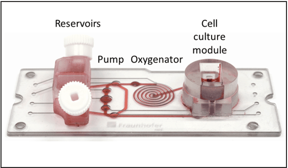
Chip for 3D cell cultures with pump and oxygenator
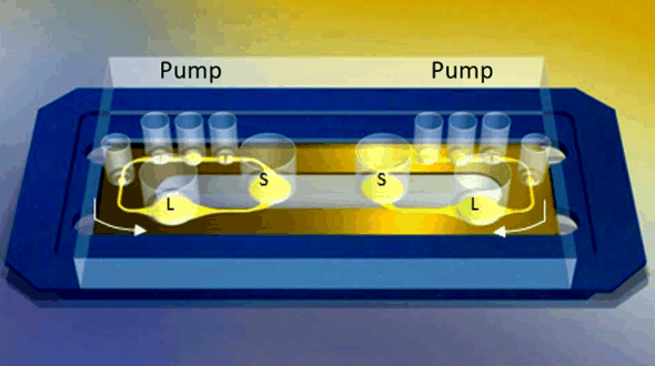
Schematic drawing of MOCs for liver and skin on a slide-sized chip with simple “blood circulation” (by integrated peristaltic pumps)
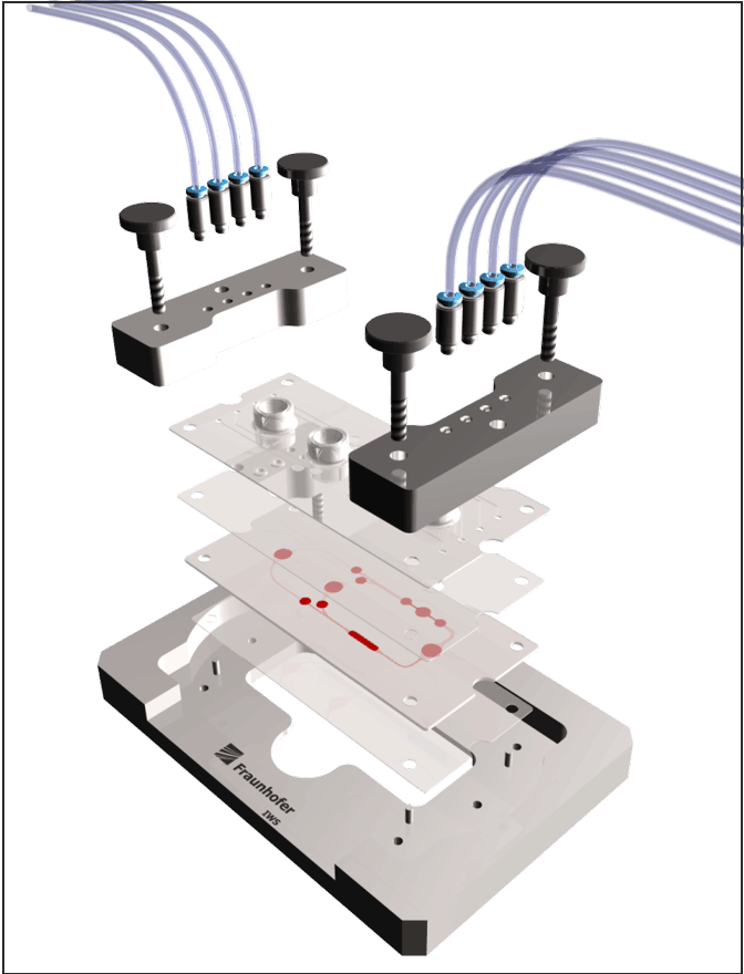
Flowthrough cell assembly
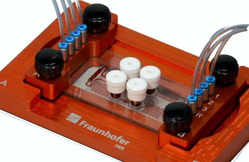
MOC ready to use (Courtesy Fraunhofer IWS and TissUse GmbH)
Alternatively you can use 12 or 24-well microwell plates into which cells, organs or cellular scaffolds are printed with the GeSiM Nano-Plotter or the BioScaffolder. Wells are covered by PDMS membranes (cast in the MicCell moulding station) that are deflected by air pressure. Nutrients, drugs or signal molecules can be added via tubes, all with automatic analysis in a microscope.
This work was conducted by
Fraunhofer IWS Dresden, TU Berlin, ProBioGen AG Berlin, GeSiM mbH
Introduction
The prototype of this “organs-on-a-chip” (OOC) platform is supposed to enable studies of the interaction of consumer-relevant synthetic or natural substances with the human body in its typical environments and with its individual genotypic specificities. It has been designed for the long-term culture of human sub-organoids in small cavities of a microfludic flow-through cell.
Design of the Multi-Bioreactor Chip
A double sided micromachined silicon chip at the size of a standard glass slide is the heart of the bioreactor. It contains the growth segments and the cavities for the stem cells. The silicon chip is than enhanced with a PDMS layer shaping fluidic structures for supply and removal of reagents.
| Features: – Standard microscope slide format | Each micro-bioreactor consists of – Three ogan growth segments |
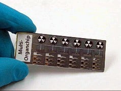
Multiorgan chip
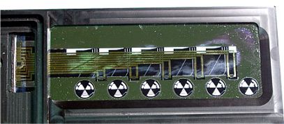
Bioreactors on the Multi-Organ-Chip
| Layer | Material | Technology | Functions | |
|---|---|---|---|---|
| 1 | PDMS (2000 µm) | Casting | Channels and reservoirs |
Cross section of the Multi-Bioreactor-Chip |
| 2 | Glass (200 µm) | Lithography, Laser | Closing layer | |
| 3 | Silicon (400 µm) | Lithography, Laser | Channels, organ growth segments & stem cell niche | |
| 4 | Glass (200 µm) | Sensors and heaters | Sensors and heaters |
The micromachining department at GeSiM contributed to the development by:
- Lithography and mask design
- Development of a new deep RIE etching process for micro patterning of silicon wafers
- Adaptation of the PDMS casting technology for the fluidic reservoirs (Layer 1)
- Development of a three layer glass/silicon/glass sandwich with embedded heater/sensor arrays (Accuracy of temperature control 0.1 K)
Instrumentation
GeSiM developed a docking station for unattended operation of the bioreactor chip. Laboratory compatibility was ensured by sticking to the common micro titer plate format (Approx. 125 mm x 83 mm). Therefore the bioreactor docking station fits to common laboratory robots, shakers, incubators, microscope stages and others.
Features:
- Data exchange with PC
- Battery based operation for at least 2 hours
- Automatic charging in the docking station
- Data acquisition and logging for at least 14 days (E.g. temperature)
- Monitoring and alerting function for limit values

